Beyond visual inspection: DEFECT REVIEW
Silicon wafers are critical and sensitive devices. Automatic loading is the only way to assure a safe and reliable handling and avoid damages.
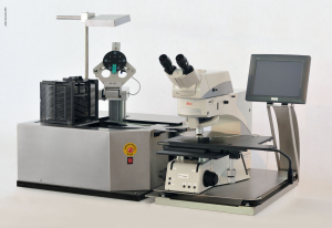
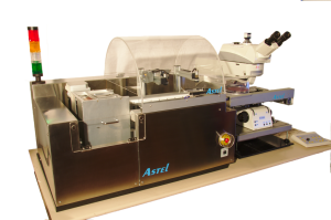
Semisyn loaders have been designed to fulfill the needs of a safe handling of any type of wafers, including the critical thin, warped, bonded or TAIKO wafers.
Visual inspection in semiconductor wafer production is often performed through automated inspection systems. Such systems needs to be integrated with a review instrument where an operator is able to validate the results of the automated inspection.
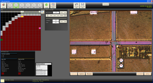
 This type of inspection is driven through wafer maps, enabling the direct access to a single die, a sequential inspection of dice, inspection of all dice, only defective or only good dice.
Bin code classification, image capture, storage and retrieval, measures and microscope management are included into the system.
Macro inspection functions are available, such as front and back inspection, with LED illuminators. Maps are downloaded and uploaded on remote server.
SECS GEM available as option.
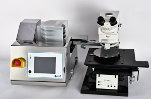
Review stations are based on RWMAP module, composed by hardware and software for microscope inspection, including motorized XY stage, camera, OCR and barcode reader.


