UV irradiation is used in semiconductor processes for a number of different reasons. The main applications are:

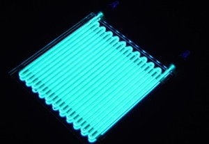
UVC irradiation lamp
UVC Ozone cleaning is a process intended to clean any kind of surface and, in particular, silicon wafers can be efficiently decontaminated by organic residues.
Wafers can also be exposed to UV-Ozone to remove resist residues or to enhance oxide thickness in epitaxial processes.
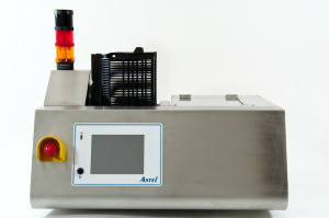
UV/Ozone system is based on high frequency UV lamps and features a controlled irradiation.
Ozone oxidizes the residues on a part surface, and UVC irradiation will produce a surface curing and decontamination.
UV is a cost effective alternative to plasma etching, since it is not required any special vacuum chamber, nor gases or special facilities.
UV deactivation for dicing and grinding tapes requires a different wavelength and is intended to deactivate the UV sensitive glue used on tapes.
Our systems for this application are based on UV tubes without ozone generation and, given the radiation wavelength, without risks for the operator.

SUE – UVC Wafer eraser
Erasing memories or other programmable devices directly on wafers is another application of UV in semiconductor production. In this case UVC radiation is used and tubes without ozone generation are mounted into our systems.
Copyright ©2021 - Astel Srl - P.IVA 07083610019
Website by Web&Com